![]() > Applications
> LD
> Applications
> LD
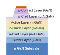
MOCVD
GaN Epitaxial
Growth
Photolithography

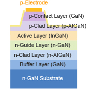
p-Electrode Formation by Sputtering
Creating p-electrode by sputtering Palladium (Pd) and Platinum (Pt)
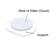
Substrate Polish
Polish away GaN substrate from the back side to be 100 µm thick
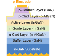
Formation of n-Electrode
Sputter Titanium (Ti), Platinum (Pt), and Gold (Au) subsequently to create n-electrode
Dicing
Cut the substrate into each chip

Dry Cleaning
Laser Diode Mount
Plasma cleaning before mounting Laser Diode chip and wire bonding

Laser Diode

![]()

![]()