
![]() > Technology
> Processes
> GaN Power Device Etching
> Technology
> Processes
> GaN Power Device Etching
As a leading supplier of GaN power device etching solutions, samco-ucp systems and process technology provide high uniformity, low damage etching with excellent etch-rate control and precision endpoint detection.
| 1) Repeatable Low-rate Etching (AlGaN: ~1nm/min) Repeatable run-to-run etch-rates from 1nm/min facilitate precise depth control. [click for details] | 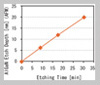 |
|
2) High GaN/AlGaN Selectivity Etching (GaN/AlGaN 100:1) Achieve etching-stop on the AlGaN interface without over-etching. [click for details] | 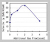 |
|
3) Precision Depth Measurement and Endpoint Detection Accurately endpoint AlGaN recess etches to the nanometer (eg 27nm etched). [click for details] |  |
![]()

![]()