


About samco-ucp
samco-ucp was founded on June 1, 2014, after Samco and UCP decided to join forces.
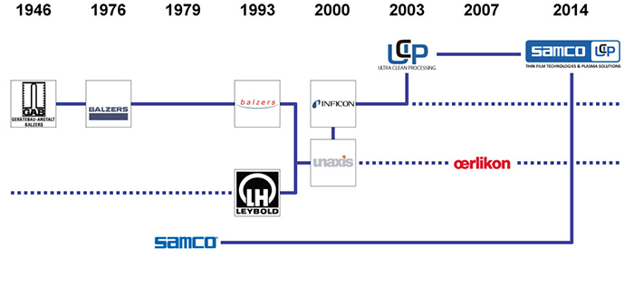
Prior to this day, both companies were already well-known in the thin film and plasma technologies.
Samco was founded in 1979 and has been primarily engaged in manufacturing thin-film deposition, etching and surface treatment process equipment for compound semiconductors, in particular applications such as LEDs and power devices. From its beginnings in a small shop in Kyoto, Japan, Samco now operates overseas offices in the USA, China, Taiwan, South Korea, and Malaysia.
The acquisition of UCP has led to the establishment of Samco’s European office.
UCP’s foundation dates back to the year 1946. Years later, the business unit “Ultra Clean” via a management buy-out, became the company “Ultra Clean Processing”, or better known as UCP. UCP has been a leading developer, manufacturer and supplier of innovative remote plasma cleaning systems.
The join forces enables samco-ucp to extend its customer support structure in the global market, while maintaining the local company culture with several decades of process knowledge and experience in the field of semiconductors and MEMS.
Located in the Heart of Europe
In between Switzerland and Austria, with a population of about 37'000 and a size of 160 square kilometers, there is the Principality of Liechtenstein. It offers easy access to all European countries and major semiconductor and MEMS industries. Since 2014 Liechtenstein is the new home of samco-ucp.

samco-ucp ltd.
Industriering 10 LI-9491 Ruggell Liechtenstein
Phone: 423-377-5959
E-mail info@samco-ucp.com
Remote Plasma Sources
samco-ucp Plasma Cleaning Systems are particularly equipped with remote plasma sources for outstanding cleaning results. In addition, the patented hydrogen process (US 6203637) is well-suited for removing various kinds of surface contaminants.

Chemical cleaning with DC plasma
The batch-type Plasma Cleaning Systems of the LFC150 family operate with a low pressure DC plasma generated by a hot filament. The patented plasma chemical cleaning process takes advantage of low-energy ions and radicals that react with surface contaminants to form volatile compounds.

Chemical cleaning with RF downstream plasma
The single substrate Plasma Cleaning System as well uses the principle of damage-free plasma chemical cleaning. The excitation of the process gas is accomplished by an RF powered hollow cathode plasma source. Remote plasma processing ensures that sensitive substrates are effectively shielded from the primary RF plasma.
Chemical vs Physical Cleaning

Chemical Plasma Cleaning
Selective removal by reaction between process gases and surface (mono) layers; very low temperature, no over etching, no redeposition (volatile reaction products) and no risk of substrate damage (strip, die, wafer).

Physical Plasma Cleaning
Mechanical removal (sputtering) by ion bombardment, typically by Ar via bias voltage: high rate, elevated temperature, over etching, redeposition (on strip and chamber) and risk of physical substrate damage (strip, die, wafer).